Nikon Corporation Unveils Cutting-Edge ArF Scanner: The NSR-S333F
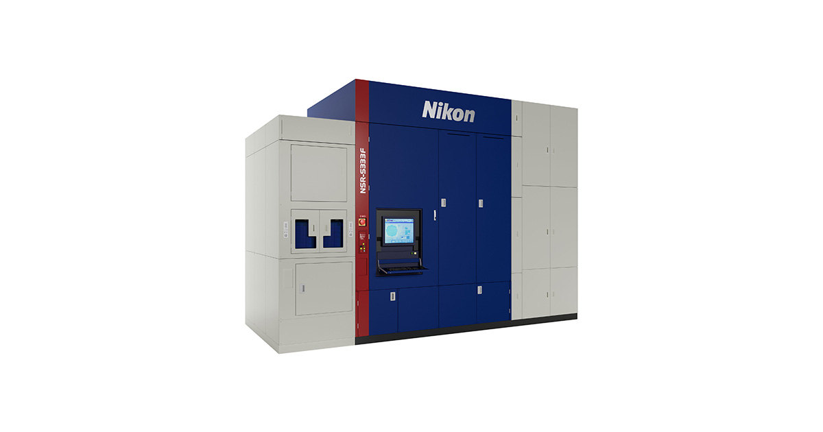
Nikon Corporation, a leader in imaging and optics, has announced the launch of its latest ArF scanner, the NSR-S333F. This new scanner is poised to set a benchmark in the industry by offering unparalleled overlay accuracy and exceptional productivity. Building upon the advanced platform of its predecessor, the NSR-S636E, and refining the proven ArF optics of the NSR-S322F, the NSR-S333F is designed to cater to the complex needs of today’s semiconductor manufacturing. Nikon plans to begin accepting orders for the NSR-S333F in October 2025, with the first deliveries anticipated in the latter half of 2026.
Development Background
The rapid advancement of technologies such as the Internet of Things (IoT) and Artificial Intelligence (AI) has led to an increased demand for more compact, high-performance semiconductor devices. Manufacturers face mounting pressure to enhance both overlay accuracy and productivity in creating advanced logic chips, next-generation memory, and high-resolution image sensors. In response to these industry demands, Nikon developed the NSR-S333F to ensure both exceptional productivity and precision accuracy.
Key Benefits
Significant Improvement in Throughput by Platform Enhancement
The NSR-S333F leverages the advanced platform of Nikon’s flagship ArF immersion scanner, the NSR-S636E. By increasing the speed of both the wafer stage and the reticle stage, this new system achieves a remarkable throughput of over 300 wafers per hour. This represents a significant leap in productivity, with the NSR-S333F delivering approximately 1.5 times higher productivity compared to its predecessor, the NSR-S322F. This enhancement in throughput is crucial for semiconductor manufacturers who aim to meet the ever-growing demands of modern technology markets.
Achieves Industry-Leading Overlay Accuracy
The NSR-S333F features improved performance in crucial areas such as wafer alignment measurement, reticle stage measurement, and autofocus. These enhancements are a result of combining the proven optical system of previous ArF scanners with the advanced platform of the ArF-S636E. As a result, the NSR-S333F delivers industry-leading overlay accuracy, with a Mix and Match Overlay (MMO) precision of less than or equal to 4 nanometers. This sets a new standard for ArF scanners in the industry, ensuring that semiconductor devices meet the highest quality standards.
Performance Overview
The NSR-S333F boasts impressive specifications that underline its cutting-edge capabilities:
- Resolution: Less than or equal to 65 nanometers
- Numerical Aperture (NA): 0.92
- Light Source: ArF excimer laser with a wavelength of 193 nanometers
- Reduction Ratio: 1:4
- Maximum Exposure Area: 26 mm x 33 mm
- Overlay Accuracy: MMO of less than or equal to 4 nanometers
- Throughput: Greater than or equal to 300 wafers per hour (96 shots)
Understanding the Technical Jargon
For those unfamiliar with the technical terms, here’s a brief explanation:
- ArF Scanner: A type of photolithography tool used in semiconductor manufacturing that uses an Argon Fluoride (ArF) excimer laser to project circuit patterns onto silicon wafers.
- Overlay Accuracy: This refers to the precision with which different patterned layers on a semiconductor wafer align with each other.
- Throughput: The number of wafers processed per hour, indicating the efficiency and speed of the scanner.
- Numerical Aperture (NA): A dimensionless number that characterizes the range of angles over which the scanner can accept or emit light. A higher NA indicates better resolution.
Reactions and Insight
The announcement of the NSR-S333F has generated significant interest in the semiconductor industry. Analysts and industry experts are optimistic about the potential impact of this new scanner on semiconductor manufacturing processes. With its enhanced throughput and overlay accuracy, the NSR-S333F is expected to meet the demands of next-generation devices that require more precise and efficient manufacturing techniques.
Some industry insiders believe that the introduction of the NSR-S333F could lead to reduced production costs for semiconductor manufacturers. By enabling faster and more accurate production of semiconductor devices, manufacturers may be able to achieve higher yields and reduce waste, ultimately lowering the cost per unit.
Conclusion
The NSR-S333F represents Nikon’s commitment to advancing the capabilities of semiconductor manufacturing equipment. With its industry-leading overlay accuracy and enhanced throughput, this new ArF scanner is poised to play a crucial role in meeting the demands of modern technology markets. Semiconductor manufacturers looking to stay competitive in an increasingly demanding industry will likely find the NSR-S333F to be an invaluable addition to their production lines.
For more information, interested parties can refer to Nikon’s official website to explore the detailed specifications and potential applications of the NSR-S333F. As Nikon continues to innovate and push the boundaries of imaging and optics, the NSR-S333F stands as a testament to the company’s dedication to excellence and precision in technology.
For more Information, Refer to this article.


