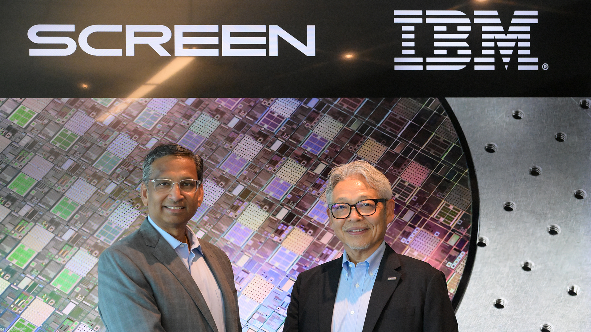
Landmark Agreement Between SCREEN Semiconductor Solutions and IBM to Advance EUV Lithography
In the ever-evolving landscape of semiconductor manufacturing, the demand for smaller and more efficient chips is unrelenting. This drive towards miniaturization has propelled Extreme Ultraviolet (EUV) lithography to the forefront of technological innovations. On September 24, 2025, SCREEN Semiconductor Solutions Co., Ltd. and IBM announced a landmark agreement to further develop cleaning processes tailored for next-generation EUV lithography, specifically focusing on High Numerical Aperture (High NA) EUV technology.
The Technological Context
For those unfamiliar, EUV lithography is a cutting-edge technology used in the fabrication of semiconductors. It utilizes light with extremely short wavelengths to etch incredibly fine patterns onto silicon wafers, which serve as the foundational building blocks for semiconductor devices. As the semiconductor industry pushes the boundaries of miniaturization, EUV lithography has become indispensable. The advent of High NA EUV represents a leap forward, promising to refine this process even further, making it possible to achieve features smaller than 2 nanometers (nm).
However, this progress introduces new challenges. In High NA EUV processes, even the tiniest particles or scratches on a wafer can significantly impair the patterning performance. As a result, the cleaning processes must be exceptionally precise and effective.
The Collaboration
Recognizing these challenges, IBM and SCREEN have joined forces to develop advanced cleaning technologies essential for High NA EUV lithography. This partnership builds on over a decade of successful collaboration between the two companies, during which they have continuously pushed the envelope in semiconductor technology. IBM brings its extensive expertise in semiconductor process integration to the table, while SCREEN contributes its state-of-the-art wafer cleaning tools.
Mukesh Khare, GM of IBM Semiconductors and VP of Hybrid Cloud, emphasized the importance of this collaboration, stating, "High NA EUV technology is critical as we look to develop smaller, more powerful semiconductors for the age of AI. We are thrilled to expand our collaboration with SCREEN to ensure that IBM and our ecosystem partners can benefit from this technology innovation."
Akihiko Okamoto, Representative Director and President of SCREEN Semiconductor Solutions, echoed this sentiment, saying, "SCREEN is excited to deepen our collaboration with IBM to develop cleaning technologies that meet the stringent demands of High NA EUV lithography. By combining SCREEN precision cleaning expertise with IBM’s full stack development flow, we aim to deliver robust solutions that enable our customers to realize the potential of sub-2nm manufacturing."
Implications for the Semiconductor Industry
This joint effort is poised to accelerate the development of advanced cleaning technologies tailored for High NA EUV lithography. The collaboration aims to provide semiconductor device manufacturers with solutions that not only meet but exceed current industry standards, maximizing the added value for these manufacturers.
The implications of this partnership extend beyond the immediate goals. As semiconductor devices become integral to a multitude of industries, from consumer electronics to automotive systems, advancements in EUV lithography and cleaning processes will have far-reaching impacts. More efficient and powerful chips will drive innovations in AI, cloud computing, and the Internet of Things (IoT), among other areas.
Background on the Companies
SCREEN Semiconductor Solutions Co., Ltd. is a prominent player in the global semiconductor market, renowned for its wafer processing equipment. The company consistently holds the leading global share in wafer cleaning equipment and provides a comprehensive range of solutions that support semiconductor production. SCREEN’s offerings include lithography, annealing, and measurement/inspection systems. Their product lineup is vast, catering to both cutting-edge devices and IoT solutions with substrates of various sizes.
IBM, a global leader in hybrid cloud and AI technology, offers consulting expertise to clients in over 175 countries. The company’s hybrid cloud platform and Red Hat OpenShift are instrumental in digital transformations across critical infrastructure sectors like financial services, telecommunications, and healthcare. IBM’s innovations in AI, quantum computing, and industry-specific cloud solutions are supported by a commitment to trust, transparency, and inclusivity.
Industry Reactions and Future Prospects
The announcement of this collaboration has been met with enthusiasm across the semiconductor industry. Industry analysts highlight the potential of High NA EUV to revolutionize chip manufacturing, enabling devices that are not only smaller but also more energy-efficient and powerful.
Looking ahead, the success of this collaboration could pave the way for further advancements in semiconductor technology. As IBM and SCREEN continue to innovate, their efforts may inspire new partnerships and technological breakthroughs, ultimately shaping the future of the industry.
In conclusion, the partnership between SCREEN Semiconductor Solutions and IBM marks a significant milestone in the journey towards more advanced semiconductor fabrication processes. By addressing the challenges of High NA EUV lithography, these two industry leaders are setting the stage for a new era of technological innovation, one that promises to transform the capabilities of electronic devices and systems worldwide.
For more information about this partnership, visit IBM’s official website here.
For more Information, Refer to this article.







![Elite gamers battle on advanced OLED displays at Samsung KX. [Photo] Inside Samsung OLED FC: Elite Gamers Compete Live on Advanced OLED Displays at Samsung KX](https://www.hawkdive.com/media/samsung-tvs-and-displays-s90f-tvs-odyssey-oled-g6-samsung-oled-fc_thumb932f-218x150.jpg)


